Showing posts with label Electronics 1 (ELE232). Show all posts

The way to care your device’s rechargeable battery


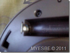
Battery is a main source for an electronic devices. Without a battery the device can still be operated by using a voltage adapter. However, when we talk about device mobility, battery is required as the source to supply voltage. There are two common battery types; dry cell battery and rechargeable battery. Dry cell is the battery that is not rechargeable and you should replace a new one once it run out of charge while rechargeable battery is the battery that is able to be recharge. Normally the price for rechargeable battery is more expensive than normal dry cell battery. Therefore we should care the battery well to prevent wasting money buying a new one and indirectly we care our electronics devices.

         battery (2)            battery (1)             battery (3)

If you wish to keep your electronic device in a long period of time, you are advised to remove the battery so that it is safe and still usable in future when you open the box. Without removing it, you will see there is something (in blue color this time) on the battery holder as shown in the lower most pictures above. What happen then? Yes…correct..your battery is no longer operate able. Hope this information is useful. Sharing is improving…

READ MORE - The way to care your device’s rechargeable battery

Answer for Solid State Devices


1. Atom is a smallest particle of an elements. Every one of the elements is made up of atoms with its own structure

2. The basic particle of negative charge is electrons while proton is the basic particle of positive charge.

3. A typical atom consist of proton, neutron and electron.

4. Atomic number is the number of proton for an atom of an elements.

5. All elements does not have the same types of atoms because every elements having their own atomic number that correspond to their number of proton. Since the number of proton equal to the number of electrons, bigger the atomic number will indicate more and more shells it has.

6. Free electron is the electron that is located in conduction band. The electron is initially located at the valance band before receiving thermal/external energy. Hence, the electron that jump from valance band to the conduction band is called free electrons.

7. Shell is a layer where the electrons seated. Every layer has their own energy level. The first layer that is the closest to nucleus is called first shell. The next shell will be 2nd, 3rd, 4th…..etc. shells.

8. Gold and Silver

9. Neutron and proton are the particles in the nucleus of an atom.

10. Valence band is also known as valence shell that is the outermost shell of an atom. In valence band, it can contain one up to eight valence electrons. If the valence electrons equal to one, it is nearly perfect conductor whereas if the valence electrons equal to eight it is insulator. So, we know that of producing an insulator the valence electrons must be equal to eight. There is a case where the valence electrons equal to four. In this case it is a semiconductor. In term of conductivity of an element, it depends on the number of electrons located in its valence band. In fact, conductivity is proportional to one and inversely proportional to the number of electrons in valence band (number of valence electron). Therefore, the higher conductivity correspond to the lesser its valence electrons and vice versa. In order to know an element is in which type, therefore we have to refer to their atomic number. Then calculate how many shell it has and how many electrons in every shell. The formula to calculate maximum number of electrons in every shell is N=2n^2, where n is the shell number.

11. For semiconductor, the electrons in their valance band is equal to four.

12. N=2n^2

n = number of shell = 4

N = 2 x (4)^2 = 2 x 16 = 32

Therefore, the maximum number of electrons in fourth shell is 32.

13. TRUE

14. Conduction band is located outside the valance band.

15. Energy level is the level of energy at a certain shell. Energy level for the outermost shell is higher than the inner shell and the innermost shell.

16. Energy gap is basically the gap of energy between two shells. It is also the amount of energy required for valence electron to jump from its valence band to the conduction band.

17. Intrinsic semiconductor is a pure semiconductor without any impurities added in.

18.

Insulator Semiconductor Conductor

The material that does not conduct electrical current in a normal condition.

The material between conductor and insulator.

The material that easily conducts electrical current.


19. Germanium only required small amount of energy to escape from their atom because it has smaller energy gap compared to silicon.

20. FALSE

21.TRUE

READ MORE - Answer for Solid State Devices

Solid State Devices – Part 1


INTRODUCTION

In this chapter, we will try to understand what does it means by solid state devices. A solid state device is basically an electronic device used in nowadays instruments and system. Solid state device is made up of semiconductor element that is either conductor or insulator. The semiconductor has useful characteristic that is suitable to work as an amplifier or rectifier.


ATOMIC STRUCTURE

Atomic structure is the first theory that we need to understand before any further discussion being made. Let us start from the top to the bottom. From the top; lets refer to the periodic table of the elements, there are more than hundred elements listed there. Every one of the elements is made up of atoms with its own structure. In atom structure, there are three basic particles that are protons, neutrons and electrons. Protons hold positive charge, neutrons hold neutral charge and electrons hold negative charge. Nucleus is the core of atom structure. In the nucleus, there is the place where proton and neutron are located. Electron however located around the nucleus on its orbit. There are a few orbits depending on elements. This orbit we called as shell. The outermost shell is called valence shell or valence band. The electrons in the valence shell are called valence electrons.


VALENCE BAND

Valence band is also known as valence shell that is the outermost shell of an atom. In valence band, it can contain one up to eight valence electrons. If the valence electrons equal to one, it is nearly perfect conductor whereas if the valence electrons equal to eight it is insulator. So, we know that of producing an insulator the valence electrons must be equal to eight. There is a case where the valence electrons equal to four. In this case it is a semiconductor. In term of conductivity of an element, it depends on the number of electrons located in its valence band. In fact, conductivity is proportional to one and inversely proportional to the number of electrons in valence band (number of valence electron). Therefore, the higher conductivity correspond to the lesser its valence electrons and vice versa. In order to know an element is in which type, therefore we have to refer to their atomic number. Then calculate how many shell it has and how many electrons in every shell. The formula to calculate maximum number of electrons in every shell is N=2n*2, where n is the shell number.


FREE ELECTRONS

Electrons orbit the nucleus of an atom at a certain distance depending on which shell it belongs to. The electrons which located at the shell that is closest to the nucleus are having lesser energy compared to the electrons located at the outermost shell. In details, more far away the electrons to the nucleus of an atom more energy it has. Every shell has their own energy level where it is getting higher and higher as it moves away from the nucleus. Based on that understanding, electrons in valence band have highest energy among all other electrons and hence whenever it gets a little more energy (plus the energy that it has) it is able to leave the valence band and become a free electron in conduction band.


CONDUCTION BAND

We knew that the outermost shell of an atom is the valence band. Conduction band is the band that is outside the valence band separated by energy gap in between them. In conduction band, electrons are having high energy that makes it very easy to be influenced by external force.


ENERGY LEVEL AND ENERGY GAP

Energy level and energy gap are two different things. Energy level is the level of energy at a certain shell whereas energy gap is the energy different between conduction band and valance band. As mentioned earlier that of energy level for the outermost shell is definitely higher than the inner shell. It is due to the attractive force, F. Energy gap in the other hand is the amount of energy required for valence electron to jump from its valence band to the conduction band.


CONDUCTOR, INSULATOR, SEMICONDUCTOR

Conductor, insulator and semiconductor are three different types of materials. Conductor material is a material that easily conducts electrical current. The atom for conductor material contains one to three valence electrons. Smaller the valence electron is better in their conductivity. The material that does not conduct electrical current in a normal condition is called insulator. Insulator has five to eight valence electrons. Almost like conductor but for insulator higher valence electron better it isolate current. The energy gap for insulator is also far distance that makes the valence electron (in valence band) difficult to travel across the energy gap. However, if the external force in not under normal condition (extremely high), possibility of the valence electron to travel beyond the energy gap is true. This will make the material conducting current but not as good as the conductor. Semiconductor is a material between conductor and insulator. It is not as good as a conductor and also not as good as an insulator. The atom for semiconductor material contains four valence electrons and it is able to conduct electrical current. Intrinsic semiconductor however is a pure semiconductor without any impurities added in.

READ MORE - Solid State Devices – Part 1

Tutorial for Solid State Devices


1. Define atom.

2. What is the basic particle of negative charge? and positive charge?

3. What does a typical atom consist of?

4. Define atomic number.

5. Do all elements have the same types of atoms? Why?

6. What is a free electron?

7. What is a shell in the atomic structure?

8. Name two conductive materials.

9. What are the particles in the nucleus of an atom?

10. Briefly explain what valence band is.

11. How many valence electrons in their valance band of a semiconductor atom?

12. What is the maximum number of electron in the fourth shell of an atom?

13. Conductivity depends on the number of electrons in conduction band. (True/False)

14. Where is the conduction band?

15. Describe energy level.

16. Describe energy gap.

17. What is intrinsic semiconductor?

18. What is the different between insulator, semiconductor and conductor materials?

19. Why Germanium only required small amount of energy to escape from their atom and become free electrons compared to the Silicon?

20. The electrons in the outermost shell having lower energy compared to the electrons in the innermost shell due to the attractive force, F. (True/False)

21. In the valence band, its contain 1 up to 8 electrons. (True/False)

READ MORE - Tutorial for Solid State Devices

Tutorials, Quizzes and Assignments

cooltext528848390
* You are not allowed to use PENCIL in your exam (Quizes, Tests and Final) except for drawing.
* Monday is a CORPORATE DAY, so you do need to wear smart attire. Lab jacket is strictly not allowed in the lecture/tutorial class.

Please download your notes from I-Learn Portal.
*Find your notes from any available folder


ShoutMix chat widget


cooltext528850803

TEST 1 (8-10AM)
10 July 2011 at Laman Perdana & Laman Siswa
Chapter 1 & Chapter 2 ONLY

TEST 2 (8-10PM)
8 September 2011 at Laman Perdana & Laman Siswa
Chapter 3, 4, 5 & 6 ONLY

ELE232 EE1113I1/I2 & EE1113D2

TUTORIALs
Your tutorial questions is here .
Your tutorial questions can be downloaded HERE .
 
QUIZzes
Please download your Quiz 1 HERE .
Due date: Tutorial Class Week 10
 
Please download your Quiz 2 HERE .
Due date: Tutorial Class Week 11
 
 
ASSIGNMENTs
Assignment 1 – Do TUTORIALs (WEEK 1 – WEEK 5)
Due date: Tutorial Class Week 12
 
Assignment 2 – Do TUTORIALs (WEEK 6 – WEEK 9)
Due date: Tutorial Class Week 13
 
Assignment 3 – Do TUTORIALs (WEEK 10 – WEEK 13)
Due date: Tutorial Class Week 14
 

NOTE: ‘0’ mark will be given for the late submission.


Carry Marks Group D2

Bil. No. Pelajar Test 1 15% Test 2 15% Q & A 10% Carry Mark
Test 1 + Test 2 = 30%
1 2010438108 8.0 11.0 x 19.0
2 2010876476 6.3 7.5 x 13.8
3 2010847444 4.3 2.8 x 7.0
4 2010618522 6.0 5.0 x 11.0
5 2010263026 4.8 11.0 x 15.8
6 2010290152 4.3 9.3 x 13.5
7 2010855112 2.3 3.0 x 5.3
8 2010893962 8.0 10.5 x 18.5
9 2010244452 3.3 0.0 x Test 2 - Unknown
10 2010449418 6.0 4.8 x 10.8
11 2010208062 4.6 0.0 x Test 2 - Unknown
12 2010213364 3.8 4.3 x 8.0
13 2010858584 5.3 9.3 x 14.5
14 2010809068 5.5 5.0 x 10.5
15 2010695692 5.3 9.0 x 14.3
16 2010808538 7.3 3.8 x 11.0
17 2010431324 3.8 8.8 x 12.5
18 2010834174 2.8 4.0 x 6.8
19 2010892466 3.5 9.8 x 13.3
20 2010841744 6.0 14.0 x 20.0
21 2010216696 6.3 1.8 x 8.0
22 2010488612 6.5 11.0 x 17.5
23 2010233354 8.5 12.5 x 21.0

“I Wish You All Good Luck For Your Final Exam”

carry marks Group I

Bil. No. Pelajar Test 1 15% Test 2 15% Q & A 10% Carry Mark
Test 1 + Test 2 = 30%
1 2010859412 7.0 5.3 x 12.3
2 2010293648 6.8 9.5 x 16.3
3 2010420658 5.3 8.0 x 13.3
4 2010840458 6.3 4.8 x 11.0
5 2010412838 4.0 3.3 x 7.3
6 2010407658 4.8 0.0 x 4.8
7 2010631998 5.8 5.0 x 10.8
8 2010458602 0.0 5.3 x 5.3
9 2010627856 4.8 13.8 x 18.5
10 2010256526 5.3 5.0 x 10.3
11 2010856506 5.8 7.5 x 13.3
12 2010281786 7.8 4.0 x 11.8
13 2010658704 9.0 10.5 x 19.5
14 2010482644 1.3 0.5 x 1.8
15 2010473442 7.8 12.3 x 20.0
16 2010282114 5.5 2.3 x 7.8
17 2010688952 7.8 12.5 x 20.3
18 2010610488 10.3 13.0 x 23.3
19 2010442086 5.0 8.5 x 13.5
20 2010660446 6.0 9.8 x 15.8
21 2010296838 4.0 4.8 x 8.8
22 2010441756 7.3 3.3 x 10.5
23 2010658974 6.8 7.5 x 14.3
24 2010660302 7.8 6.0 x 13.8
25 2010233552 8.8 4.0 x 12.8
26 2010814322 12.8 12.8 x 25.5
27 2010884426 5.5 6.0 x 11.5
28 2010275138 8.3 7.5 x 15.8
29 2010865482 8.3 11.5 x 19.8
30 2010417824 9.0 9.8 x 18.8
31 2010888978 4.8 7.8 x 12.5
32 2010640784 5.5 6.0 x 11.5

 “I Wish You All Good Luck For Your Final Exam”


ELE232 C1/C2

Please download your Assignment 1 here .
Ans: 1) i) 2.5V ii) 22.75V iii) 3.17% 2) Diode pointing down & VDC 4.7V
NEW Surprised smile Please download your Quiz 2 here .
NEW Surprised smile Please download your Quiz 3 here .
NEW Surprised smile Please download your Quiz 4 here .


cooltext528852666

image

EEE231 EE1123D1/D2

TUTORIALs
Your tutorial questions can be downloaded HERE .
 
QUIZzes
Please download your Quiz 1 HERE .
Due date: Tutorial Class Week 10
 
Please download your Quiz 2 HERE .
Due date: Tutorial Class Week 13
 
 
ASSIGNMENTs
Assignment 1 – Do TUTORIALs (WEEK 1 – WEEK 5)
Due date: Tutorial Class Week 11
 
 
Assignment 2 – Do TUTORIALs (WEEK 6 – WEEK 9)
Due date: Tutorial Class Week 12
 
 
Assignment 3 – Do TUTORIALs (WEEK 10 – WEEK 13)
Due date: Tutorial Class Week 14
 

NOTE: ‘0’ mark will be given for the late submission.


Carry Marks

Bil. No. Pelajar Test 1 15% Test 2 15% Q & A 10% Carry Mark
Test 1 + Test 2 = 30%
1 2010441674 7.3 5.8 x 13.0
2 2010218772 6.3 6.8 x 13.0
3 2008310191 5.0 0.0 x 5.0
4 2010295514 7.0 6.5 x 13.5
5 2010643524 8.0 9.0 x 17.0
6 2010652938 7.3 8.8 x 16.0
7 2009263488 8.3 10.5 x 18.8
8 2009897152 8.3 10.5 x 18.8
9 2010819988 15.0 13.5 x 28.5
10 2010847688 12.8 11.3 x 24.0
11 2010428372 10.0 10.8 x 20.8
12 2010609246 10.8 13.0 x 23.8
13 2010451966 7.8 10.5 x 18.3
14 2010426026 6.5 12.3 x 18.8
15 2010861776 11.5 11.8 x 23.3
16 2010849766 11.5 12.5 x 24.0
17 2010290242 10.8 11.5 x 22.3
18 2010805644 5.8 8.3 x 14.0
19 2009855576 5.5 9.0 x 14.5
20 2010819338 7.8 7.5 x 15.3
21 2010456402 9.0 12.8 x 21.8
22 2010875888 5.8 9.8 x 15.5
23 2009678552 9.3 12.0 x 21.3
24 2010441622 12.5 11.5 x 24.0
25 2010868928 6.0 8.0 x 14.0
26 2010636228 11.0 12.8 x 23.8
27 2010451894 11.5 10.5 x 22.0
28 2010676232 5.8 10.5 x 16.3
29 2009823102 4.5 0.0 x 4.5
30 2010808672 8.5 8.8 x 17.3
31 2010808192 12.3 9.8 x 22.0
32 2009765623 6.8 7.8 x 14.5

“I Wish You All Good Luck For Your Final Exam” 


cooltext528851752

NEW Surprised smile Please download your LET’s PLAY questions here .

NEW Surprised smile Please download your Supernode Nodal answer here .

EEE121 R1/R2


Please download your Quiz 1 questions here .
Please download your Quiz 2 questions here .
NEW Surprised smile Please download your Quiz 3 questions here .
NEW Surprised smile Please download your Quiz 4 questions here .
NEW Surprised smile Please download your Assignment 1 questions here .

EEE121 K1/K2


Please download your Quiz 2 questions here .

NEW Surprised smilePlease download your Quiz 3 questions here .

NEW Surprised smilePlease download your Quiz 4 questions here .

NEW Surprised smile Please download your Assignment 1 questions here .

READ MORE - Tutorials, Quizzes and Assignments

Related Posts Plugin for WordPress, Blogger...


Total Pageviews

Advertisements

Cool Text: Logo and Graphics Generator
Home